
In modern electronics manufacturing, the PCB assembly process plays a vital role in determining overall equipment performance, dimensional footprint, and operational stability. When designing circuit boards, hardware engineers frequently weigh two primary manufacturing technologies: SMT (surface mount technology) and DIP (dual in-line package / through-hole technology). Understanding the distinct technical characteristics and mechanical strengths of each method helps enterprises select the right production strategy, balance manufacturing budgets, and enhance finished product reliability.
Technological differences between surface mount technology (SMT) and through-hole soldering (DIP)
SMT and DIP represent two generations of circuit board assembly characterized by fundamentally different component positioning mechanics:
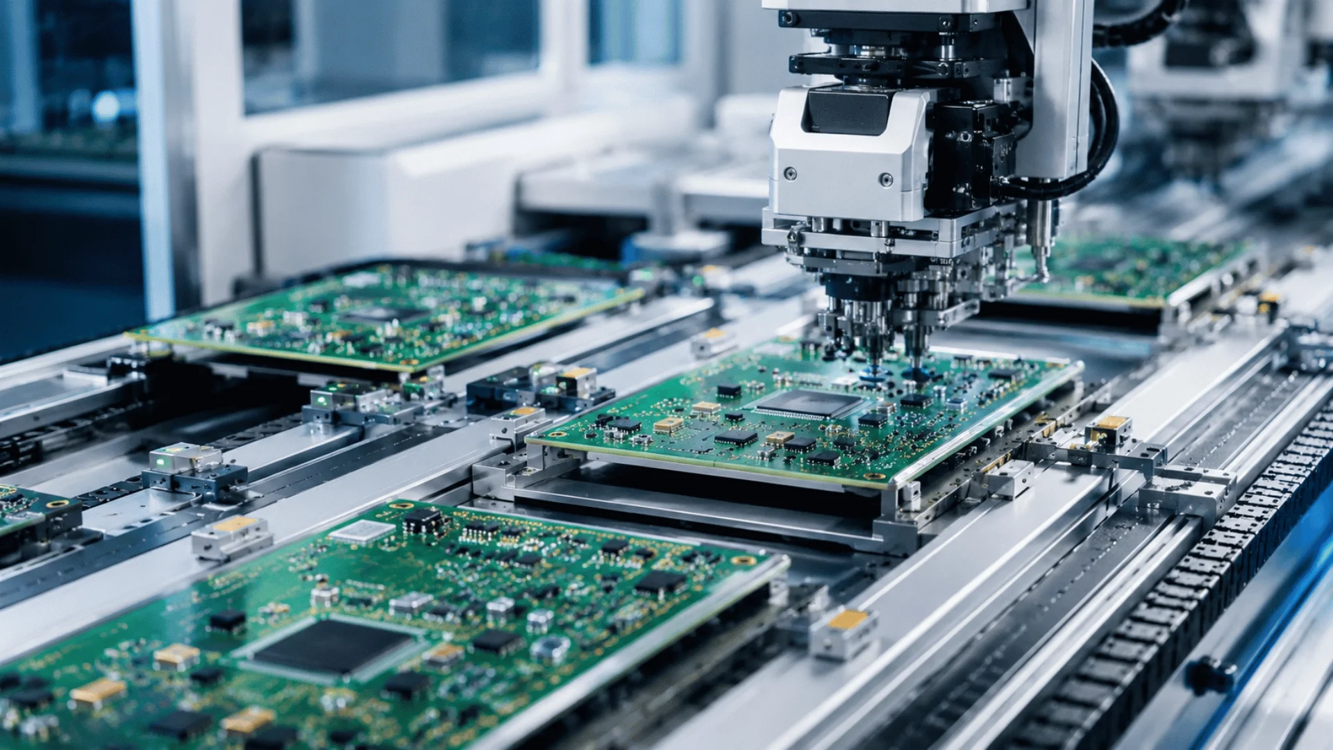
– SMT technology: Surface-mount devices (SMDs) are placed directly onto conductive copper landing pads on the board surface without drilling through-holes across the PCB substrate. After solder paste stencil printing, components are mounted automatically and routed through a multi-zone convection reflow oven to melt the alloy paste, forming durable mechanical and electrical joints.
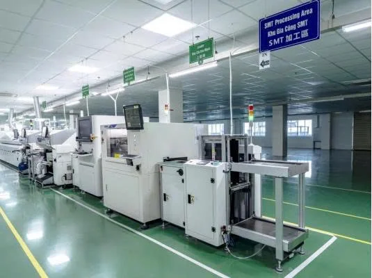
– DIP technology: Component wire leads pass through pre-drilled, copper-plated through-holes in the board and are subsequently secured using wave soldering baths or manual soldering stations on the reverse side.
The rapid evolution of consumer electronics and industrial automation has driven the PCB assembly sector predominantly toward SMT, satisfying demands for product miniaturization and expanded board functionality.
Outstanding technical advantages of SMT technology
Compared to traditional through-hole methods, SMT delivers distinct engineering improvements and production scalability:
• High component density and compact footprint: SMD packages are significantly smaller than equivalent DIP parts. Because through-hole drilling is eliminated for individual leads, manufacturers can mount components across both sides of the substrate (double-sided assembly). This substantially shrinks overall board area and reduces equipment weight while maintaining complex circuit architectures.
• Automated production speed and high throughput: The entire SMT line operates automatically via high-speed pick-and-place equipment. These machines accurately place tens of thousands of components per hour with tight repeatability. This automated throughput shortens order lead times, lowers manual labor overhead, and minimizes defects caused by operator handling.
• Signal integrity and mechanical reliability: Because SMT components feature ultra-short terminations or leadless ball arrays, parasitic resistance and trace lead inductance are reduced significantly. Consequently, SMT boards operate with higher stability across high-frequency bands, suppressing RF signal interference. Additionally, low-profile surface bonding withstands physical vibration and mechanical shock better in demanding field environments.
When should your business choose SMT or combine it with DIP?
Although SMT offers significant advantages, DIP retains unique technical value in specific applications:
| Evaluation criteria | SMT technology | DIP technology |
|---|---|---|
| Board dimensions | Highly compact, supports double-sided placement | Bulkier, requires drilled through-hole spacing |
| Automation level | Fully automated, high placement speeds | Frequently requires manual pin insertion |
| Mechanical shear strength | Moderate, ideal for low-mass components | Extremely high due to through-board lead anchoring |
| Initial setup expenditure | Requires dedicated placement lines and stencils | Simpler and more flexible for small prototype batches |
• When to prioritize SMT: Ideal for smart control boards, IoT hardware, telecommunications equipment, computer peripherals, and products demanding high routing density and slim enclosures.
• When to specify DIP: Heavy-duty power assemblies such as power transformers, high-capacitance electrolytic capacitors, industrial power relays, or external interface connectors subjected to recurring mechanical mating cycles. Through-hole joints deliver superior pull-out strength compared to surface-mount pads.
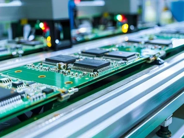
• Hybrid assembly approach: In many PCB assembly programs, the optimal solution integrates both technologies. The production line populates fine-pitch surface-mount parts via SMT first, then transfers boards to DIP stations to insert high-stress power components. This combined workflow balances high routing density with mechanical joint ruggedness at key interconnect points.
Reliable PCB assembly services at Zeng Hsing
Zeng Hsing delivers turnkey PCB assembly and OEM/ODM manufacturing solutions backed by modern facilities, flexibly accommodating both SMT and DIP technologies under rigorous engineering standards. Our automated machinery and disciplined quality control frameworks ensure high precision while optimizing total production costs for our partners. For technical consultations or detailed manufacturing quotations, please contact Zeng Hsing directly via hotline (+84) 0355 846 965 or visit our website at zenghsing.vn for prompt engineering support.
GET THE BEST QUOTE
Contact ZENG HSING now via Zalo or Website to receive advice on suitable specifications and get a prompt quotation!
ZENG HSING VIET NAM
- Address: Unit 03-08, Canary Plaza, Binh Duong Boulevard, Binh Hoa Ward, Ho Chi Minh City, Vietnam
- Hotline: (+84) 0355 846 965 (Mr. Nghia) – (+84) 0362 476 478 (Mr. Nam)
- Email: nghia_duong@zenghsing.com.vn / nam_vu@zenghsing.com.vn
- Website: zenghsing.vn

