
Electronic circuit boards serve as the operational foundation for modern technology hardware. High-quality PCB assembly requires a precise balance between automated mechanical equipment and appropriate component mounting methods. Understanding the technical differences between surface-mount technology and through-hole soldering enables engineering and procurement teams to select an efficient manufacturing strategy.
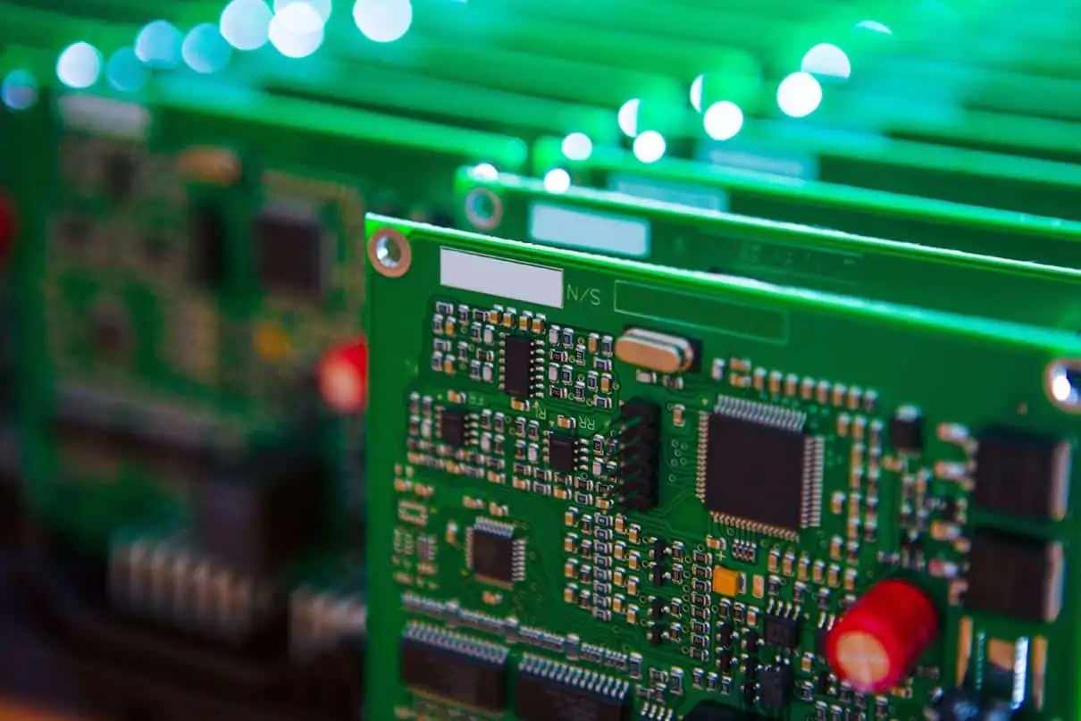
Understanding PCB assembly in electronics manufacturing
A bare printed circuit board initially functions purely as an insulated dielectric substrate patterned with etched copper conductive traces. This substrate cannot execute any signal processing or logical control tasks without mounted electronic components.
PCB assembly (Printed Circuit Board Assembly) is the technical process of mechanically fastening and electrically interconnecting discrete parts—such as resistors, capacitors, inductors, transistors, and integrated circuits (ICs)—onto a bare board according to circuit schematics. This process demands tight precision to create continuous electrical signal paths, ensuring equipment operates reliably over extended operating lifecycles. A compliant solder joint prevents open circuits and short circuits while withstanding mechanical vibration and thermal cycling in real-world environments.
Modern production workflows rely on two primary mounting and soldering methodologies: surface-mount technology and through-hole technology. Each technique offers distinct mechanical characteristics suited to specific hardware applications.
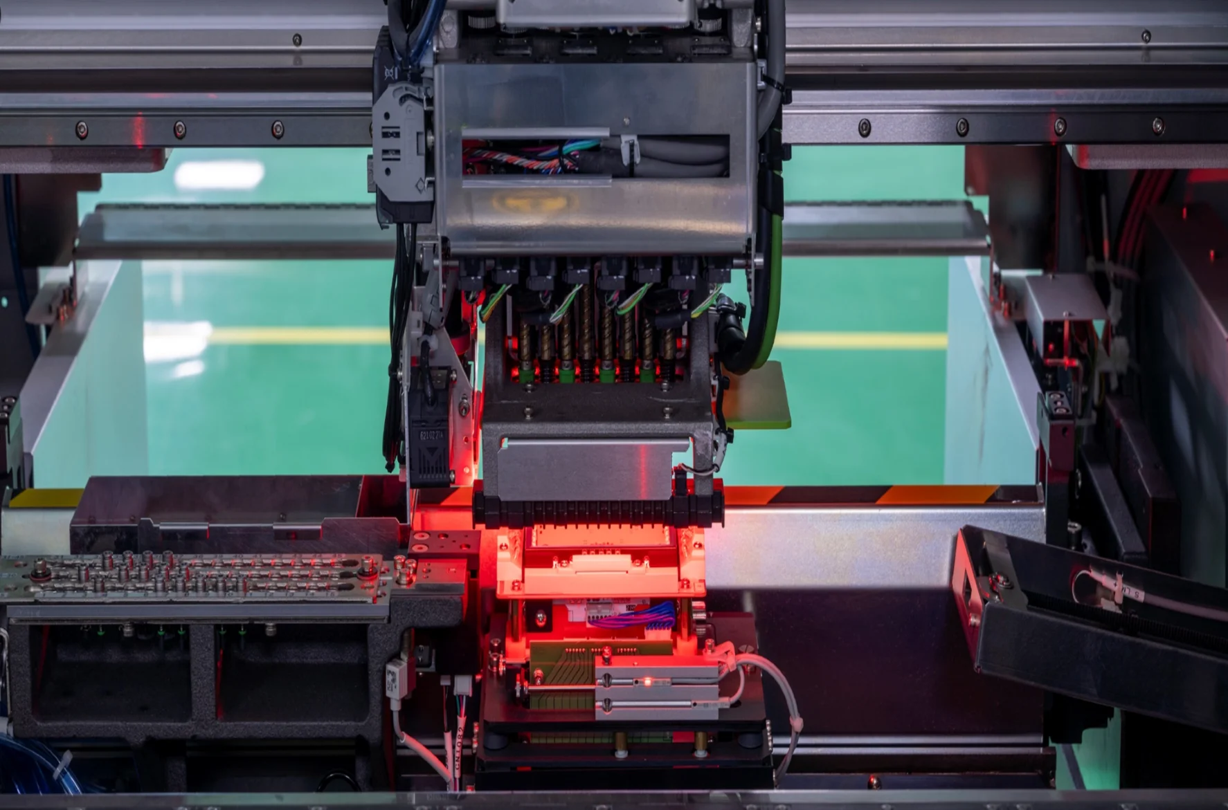
Comparing surface-mount technology and through-hole soldering
The primary distinction between both approaches lies in how components are positioned on the board substrate and how solder alloy is thermally reflowed.
Surface-mount technology (SMT)
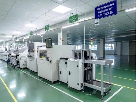
In this PCB assembly process, miniature surface-mount devices (SMDs) are placed directly onto flat copper landing pads on the substrate surface. Prior to component placement, solder paste containing alloy powder and flux is applied through a laser-cut stencil. Automated high-speed pick-and-place nozzles position components onto designated coordinates, after which the entire board passes through a multi-zone convection reflow oven. Controlled thermal profiles melt the solder paste, forming solid metallurgical bonds between component terminations and copper pads.
• Advantages: Compact component packages minimize board real estate, enabling double-sided placement to maximize circuit routing density. Fully automated assembly via high-speed equipment accelerates production cycles for high-volume manufacturing runs.
• Limitations: Requires high-resolution automated optical inspection (AOI) equipment. Manual rework or repair using hand soldering irons requires precise handling due to miniature component pitches.
Through-hole technology (DIP / THT)
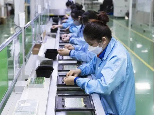
In contrast to surface mounting, through-hole assembly requires pre-drilled, copper-plated through-holes across the circuit board. Components are typically larger and feature metallic wire leads that pass through holes from the top surface to the bottom side. Protruding lead ends are then passed over a molten wave soldering bath or secured manually by soldering technicians.
• Advantages: Robust mechanical anchoring because leads extend completely through the board core. Solder joints resist high shear stresses, physical shock, and elevated thermal dissipation, providing stable current carrying capacity for high-power circuits.
• Limitations: The drilling process adds tooling steps and costs to bare board fabrication. Component insertion typically occupies single-side real estate, limiting overall board miniaturization.
Selecting the right soldering technique for your hardware design
Selecting the appropriate soldering methodology depends primarily on expected operating environments, electrical power loads, and product enclosure constraints.
When to prioritize surface-mount technology?
Surface mounting is the optimal choice for hardware designs prioritizing compact footprints, low weight, and portable mobility—such as smartphones, tablets, smart wearables, handheld medical monitors, or automotive electronic control modules. It also provides the lowest per-unit assembly cost for mass-volume runs requiring fast placement speeds.
When to prioritize through-hole technology?
Through-hole PCB assembly is suited for bulky components or interfaces exposed to recurring mechanical stresses, such as DC power jacks, terminal blocks, heavy-gauge wire connectors, high-frequency pulse transformers, large filter capacitors, and industrial control relays.
Practical mixed assembly approach: Most complex circuit boards today utilize a hybrid approach. Manufacturing lines prioritize automated surface mounting for fine-pitch control ICs and passive chips to optimize layout density, while utilizing through-hole soldering for power components and external connectors to preserve mechanical ruggedness.
GET THE BEST QUOTE
Contact ZENG HSING now via Zalo or Website to receive advice on suitable specifications and get a prompt quotation!
Optimize circuit board assembly quality with Zeng Hsing
Understanding the engineering trade-offs of each soldering technology helps businesses specify the proper production workflow, prevent unnecessary scrap costs, and control final build quality. You can consult directly with the technical engineering staff at Zeng Hsing to determine an optimal PCB assembly plan tailored to your design drawings, ensuring clean solder joints, mechanical durability, and competitive manufacturing costs.
ZENG HSING VIET NAM
- Address: Unit 03-08, Canary Plaza, Binh Duong Boulevard, Binh Hoa Ward, Ho Chi Minh City, Vietnam
- Hotline: (+84) 0355 846 965 (Mr. Nghia) – (+84) 0362 476 478 (Mr. Nam)
- Email: nghia_duong@zenghsing.com.vn / nam_vu@zenghsing.com.vn
- Website: zenghsing.vn

